
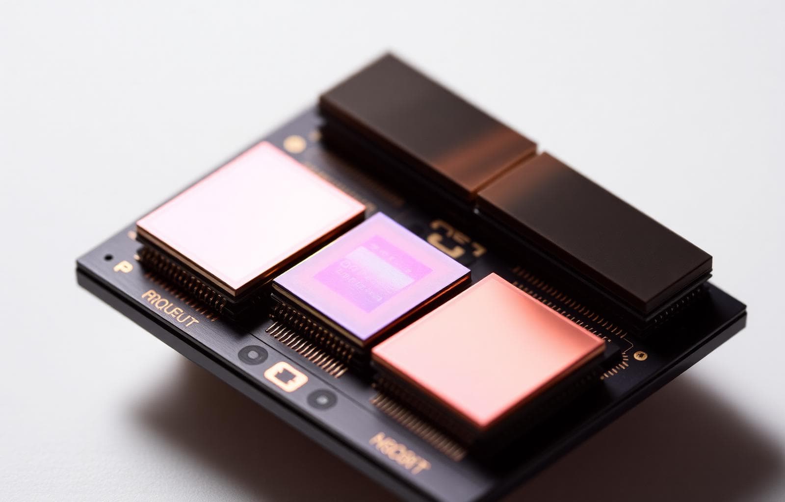
Advanced Packaging
Chiplet, 2.5D, and 3D IC Packaging Engineers
Advanced packaging is where Moore's Law scaling happens now. Chiplet, 2.5D, and 3D IC is a distinct discipline at Game 7, with its own engineering pool and its own staffing profile.
What they do
Chiplet Integration from Architecture Through OSAT Release
Advanced packaging engineers at Game 7 have designed 2.5D silicon interposer and 3D stacked-die packages for AI accelerators, HPC CPUs, and HBM-integrated systems. They understand both the electrical design (signal integrity through high-density interposer routing) and the physical design (bump map, warpage, CTE management).
They co-design with OSATs (ASE, Amkor, JCET) early. Baking in assembly design rules upfront rather than discovering them during pilot build.
Scope of work
- Package substrate design and stackup definition for flip-chip and advanced packaging platforms
- 2.5D/3D integration: silicon interposer design, TSV planning, and die-to-die routing
- Chiplet disaggregation architecture: bump map definition and die-to-die interface planning (UCIe, BoW, AIB)
- Package-level SI/PI: S-parameter extraction and IBIS-AMI analysis for package interconnect
- HBM integration: PHY interface design, thermal stack modeling, and interposer routing
- DFM coordination with OSAT (ASE, Amkor, JCET): bump pitch, underfill, and assembly process constraints
- Co-design with PCB SI team: package-to-board interface, BGA fanout, and via stub optimization
- Thermal and mechanical analysis: CTE mismatch, warpage modeling, and thermal resistance stack
Tools & Technologies
The stack our Advanced Packaging engineers actually ship in.
Program context
Where Moore's Law Scaling Happens Now
When transistor scaling slows, packaging picks up the slack. Chiplet architectures. Disaggregating a monolithic SoC into multiple smaller dies connected by a silicon interposer or advanced organic substrate. Have become the dominant strategy for AI accelerators, high-performance CPUs, and high-bandwidth memory integration. TSMC CoWoS, Intel EMIB, Samsung X-Cube, and the emerging UCIe standard are reshaping how chips are designed from the first architecture meeting. Package engineers who understand both the electrical design and the physical design are among the scarcest specialists in the industry.
FAQ
Common Questions on Advanced Packaging Staffing
What's the difference between traditional flip-chip packaging and 2.5D/3D packaging?+
Traditional flip-chip packages a single die onto a substrate using solder bumps. 2.5D packaging places multiple dies side-by-side on a silicon interposer with fine-pitch through-silicon vias (TSVs), enabling much higher bandwidth between dies than is possible through a package substrate or PCB. 3D stacking places dies vertically with TSVs through active silicon. The bandwidth density difference is enormous: a PCB trace carries a few Gbps; HBM stacked through a CoWoS interposer delivers 1+ Tbps.
Why are chiplet architects and advanced packaging engineers in such high demand?+
Two converging forces: AI compute demand and the slowdown of classical transistor scaling. Training and inference workloads require memory bandwidth that traditional monolithic SoC designs cannot provide cost-effectively. Disaggregating compute dies from memory dies (HBM), I/O dies, and specialized accelerators. Connected through advanced packaging. Is the architectural path that AMD, Intel, NVIDIA, and every hyperscaler custom silicon team is pursuing. The engineers who can design, validate, and manufacture these multi-die packages are rare because the discipline is new enough that there is no large established talent pool.
What is UCIe and why does it matter for packaging engineers?+
UCIe (Universal Chiplet Interconnect Express) is an emerging open industry standard for die-to-die electrical interfaces within a package. Analogous to what PCIe did for board-level connectivity, UCIe aims to enable chiplets from different vendors to be combined in a single package with a standardized high-bandwidth, low-latency interface. Packaging engineers working on UCIe-compliant designs need to understand the physical layer electrical specification, the bump pitch and landing pad requirements, and how UCIe interfaces to the PHY silicon.
What is the OSAT relationship in advanced packaging programs?+
OSAT stands for Outsourced Semiconductor Assembly and Test. Companies like ASE Group, Amkor, JCET, and Powertech that physically assemble and package chips after wafer fabrication. For advanced packaging programs, the package engineer works with the OSAT early in design to understand assembly design rules: minimum bump pitch, underfill dispensing tolerances, warpage limits, and stacking bond process constraints. Package engineers who have done this co-design loop before accelerate programs significantly.
Related disciplines
Cross-Links Across the Team
Floorplan, P&R, STA, and Signoff Engineers for Advanced Process Nodes
Back-end engineers who handle die-side bump and RDL preparation.
PCB Layout Engineers →High-Speed PCB Layout Engineers: DDR5, SerDes, RF
Board-side designers for BGA fanout and package-to-board channel design.
Analog & Mixed-Signal Design →Custom Analog IC and Mixed-Signal Designers
SerDes and PHY designers whose I/O circuits interface through the package.
Let's talk
Need an Advanced Packaging Engineer?
Tell us the program. We'll send a shortlist of 2-4 qualified engineers within days.