
Physical Design Engineers
Floorplan, P&R, STA, and Signoff Engineers for Advanced Process Nodes
Full-custom and standard-cell physical design for sub-5nm ASIC and SoC programs. Principal physical design engineers with Synopsys and Cadence flow experience and tape-out signoff credentials.
What they do
Physical Implementation from Floorplan Through Tape-Out Signoff
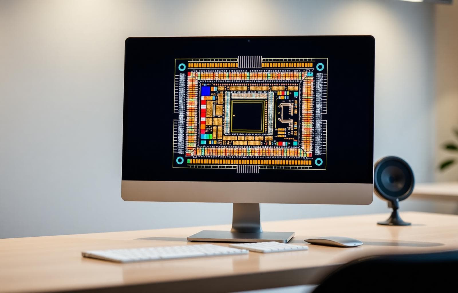
Principal physical design engineers at Game 7 have closed timing, power, and physical verification on complex SoC blocks at advanced nodes. They haven't just run the tools. They make floorplan architecture decisions, set PD methodology, manage multi-corner STA closure across PVT, and own the GDS delivery.
At 5nm and below, they've dealt with multi-patterning constraints, FinFET layout rules, increased hold sensitivity, and the complexity of delivering clean physical verification sign-off to the foundry.
Scope of work
- Chip and block floorplanning with power distribution network (PDN) and I/O planning
- Place and route for high-performance, low-power, and area-constrained designs
- Static timing analysis (STA) and multi-corner timing closure across PVT corners
- IR drop and electromigration (EM) analysis and closure using RedHawk or Voltus
- Physical verification (DRC, LVS, ERC) using Calibre and Assura
- Clock tree synthesis (CTS) for high-fanout, skew-sensitive designs
- Multi-patterning and advanced node layout constraint management (FinFET, GAAFET)
- Tape-out signoff and GDSII delivery
Tools & Technologies
The stack our PD engineers actually ship in.
Program context
Advanced Node PD, Staffed by Engineers Who've Shipped It
Physical design complexity scales dramatically with process node. At 28nm, most experienced engineers can close a block. At 5nm and below, you're managing FinFET layout rules, coloring constraints for multi-patterning, aggressive power density, and STA sensitivity to small PDN variations.
AI chip PD engineers are optimizing for power delivery to dense MAC arrays under high switching activity. Networking ASIC PD engineers are closing timing on 400G+ SerDes interfaces. Our physical design engineers have worked at these nodes and at this complexity level.
FAQ
Common Questions on Physical Design Engineers Staffing
What does a physical design engineer actually own on a SoC program?+
At the principal level, a PD engineer owns a block or subsystem from post-synthesis netlist through GDSII delivery. That means: floorplanning the block within the chip context, running and optimizing P&R, closing multi-corner STA, analyzing and fixing IR drop and EM violations, running physical verification (DRC/LVS) with Calibre, and delivering a clean GDS that meets the foundry sign-off criteria.
What process nodes do your physical design engineers have experience with?+
We have engineers with tape-out sign-off experience at 28nm, 16nm, 12nm, 7nm, 5nm, and 3nm. For sub-5nm work specifically, we ask about multi-patterning experience, FinFET layout rule familiarity, and whether the engineer has navigated advanced node DRC/LVS closure rather than just running the tools on simpler nodes.
Can Game 7 place STA engineers separately from full PD engineers?+
Yes. Static timing analysis is frequently staffed as a dedicated role on large SoC programs, particularly during tape-out crunch. STA-focused engineers who specialize in multi-corner, multi-mode timing closure using PrimeTime or Tempus are a distinct profile from full P&R engineers, and we staff both.
What's the engagement model: block-level, chip-level, or both?+
Both. Some programs need a block-level PD engineer to own a specific subsystem (PCIe interface, memory controller). Others need chip-level PD engineers who manage floorplan and top-level integration. We ask about the program structure upfront and match accordingly.
Related disciplines
Cross-Links Across the Team
SystemVerilog RTL Designers with Tape-Out Experience
RTL-to-synthesis handoff that enables cleaner PD closure.
DFT Engineers →Design for Test Engineers with Chip-Level DFT Ownership Experience
Scan-aware floorplanning and physical DFT sign-off.
Design Verification Engineers →UVM Architects and DV Leads with Verification Closure Experience
Completing the front-to-back SoC team.
Let's talk
Need a Physical Design Engineer?
Tell us the program. We'll send a shortlist of 2-4 qualified engineers within days.