
Silicon Validation
Post-Silicon Validation Engineers
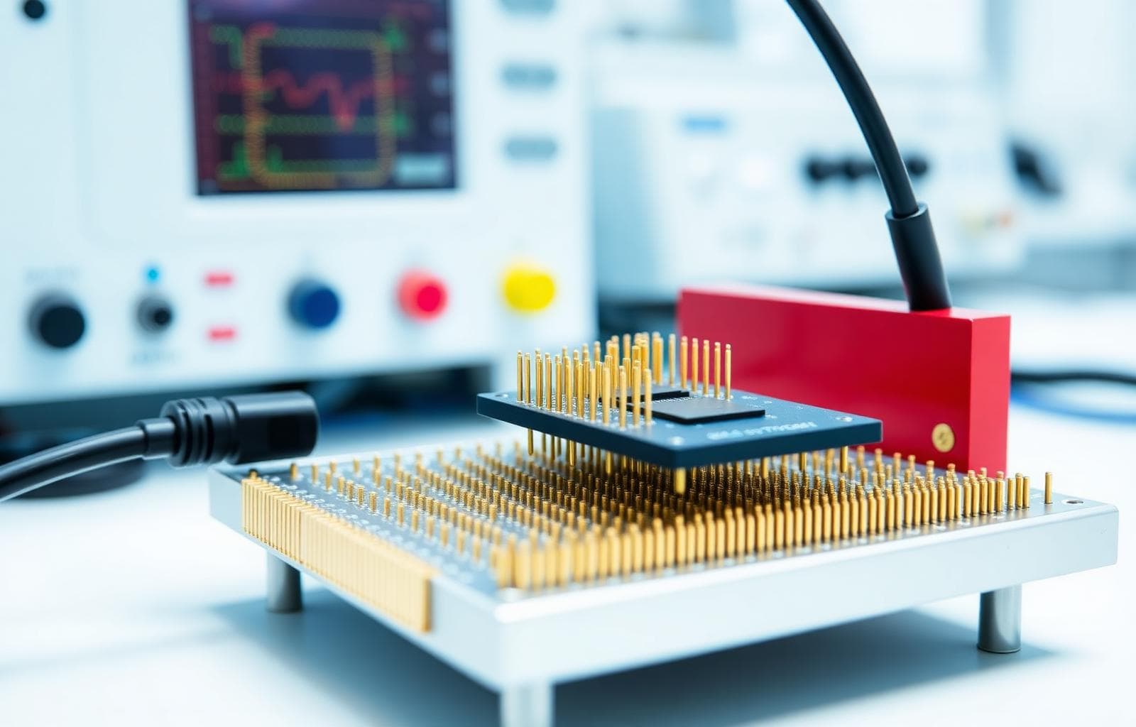
Silicon comes back from the fab and nothing works. This is the moment you need a post-silicon engineer. We've placed them on Tesla SoC programs and LAM Research board bring-ups.
What they do
Bring-Up, Debug, and Tape-Out Correlation
Post-silicon validation engineers at Game 7 have brought up SoC silicon on validation boards using JTAG, scope, and logic analyzer. Combining deep hardware knowledge with software debugging instinct.
They work with RTL, DV, PD, and DFT teams to isolate failures, file bugs, and drive root cause analysis. Often under tape-out-respin time pressure.
Scope of work
- First silicon bring-up: power sequencing, clock initialization, and boot sequence validation
- Debug of silicon failures using JTAG, oscilloscope, logic analyzer, and ATE pattern correlation
- Functional validation of SoC subsystems against RTL golden models and architectural specifications
- Performance characterization: frequency, power, and I/O margin measurement across PVT corners
- DFT-to-silicon correlation: ATPG pattern debugging and stuck-at/transition fault analysis on ATE
- Failure analysis coordination: SRAM bit-cell failures, timing failures, and IP bring-up issues
- Test program development and ATE platform bring-up (Teradyne UltraFLEX, Advantest V93000)
- Bug filing and cross-functional debug: working with RTL, DV, PD, and DFT teams on root cause
Tools & Technologies
The stack our Silicon Validation engineers actually ship in.
Program context
The Moment You Need a Post-Silicon Engineer
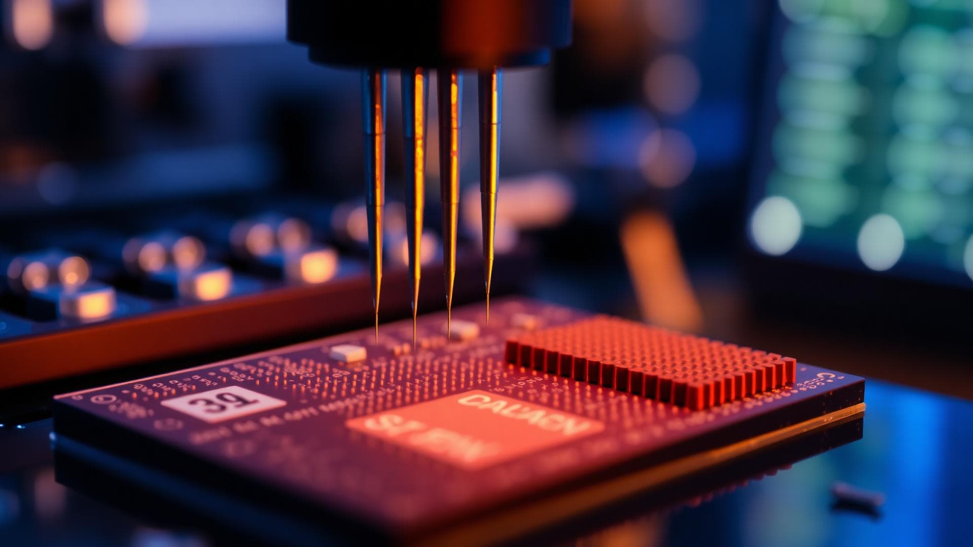
Post-silicon validation is the phase where months of RTL, DFT, and PD work meet reality for the first time. Bring-up is notoriously difficult because the silicon often does not behave as simulated. Power supply noise, manufacturing variation, test escape bugs, and subsystem interaction effects all appear together, with no documentation and limited debug visibility. Engineers who thrive here combine deep hardware knowledge (read schematics, probe boards, interpret DFT failure signatures) with software debugging instinct and the patience to work through a problem that may take days to isolate.
FAQ
Common Questions on Silicon Validation Staffing
What's the difference between a silicon validation engineer and a design verification engineer?+
Design verification engineers work pre-silicon. In simulation, emulation, and FPGA prototyping environments, verifying that RTL matches the specification. Silicon validation engineers work post-silicon. With actual fabricated hardware. A DV engineer has full visibility into every signal in the design. A silicon validation engineer has whatever test pins were designed in, whatever JTAG access the DFT team provided, and whatever the oscilloscope can see on the board. Post-silicon debug is detective work. Pre-silicon DV is systematic verification.
How early in a program should Game 7 engage for silicon validation?+
Ideally before tape-out. The validation plan. What tests to run, what measurements to take, what pass/fail criteria define a good die. Should be developed in parallel with the design. Engineers brought in at bring-up with no context on the DFT coverage plan, the scan access strategy, or the ATE test program state face an avoidable ramp-up problem. For programs where we have already placed DFT or DV engineers, transitioning those engineers into the validation phase is often the most efficient path.
Can Game 7 place ATE test program development engineers?+
Yes. ATE test program development is a distinct skill set. Writing and debugging test programs for Teradyne UltraFLEX, J750, or Advantest V93000 platforms. These engineers bridge the DFT simulation world and the production test floor. They know how to convert ATPG patterns from simulation format (STIL/WGL) to ATE-ready programs, debug correlation failures between simulation and silicon, and optimize test time for manufacturing economics.
What makes a strong post-silicon validation engineer. Technically?+
Three things: hardware fluency. Comfort with instruments (oscilloscope, logic analyzer, VNA) and the ability to read a schematic and probe the right test point. DFT knowledge. Understanding scan chains, BIST results, and what DFT coverage gaps mean for the failures you are seeing. And cross-functional communication. Bringing RTL, DV, PD, and manufacturing teams to the same table around a silicon failure and facilitating root cause analysis.
Related disciplines
Cross-Links Across the Team
Design for Test Engineers with Chip-Level DFT Ownership Experience
Scan and BIST infrastructure that post-silicon validation depends on.
Design Verification Engineers →UVM Architects and DV Leads with Verification Closure Experience
Pre-silicon verification whose coverage model informs post-silicon debug.
Hardware Engineers →Board Hardware Engineers from Schematic to Bring-Up
Board engineers who deliver the validation platforms silicon comes up on.
Let's talk
Need a Silicon Validation Engineer?
Tell us the program. We'll send a shortlist of 2-4 qualified engineers within days.