
How to Hire a High-Speed PCB Engineer (4-Layer Skills Won't Cut It)
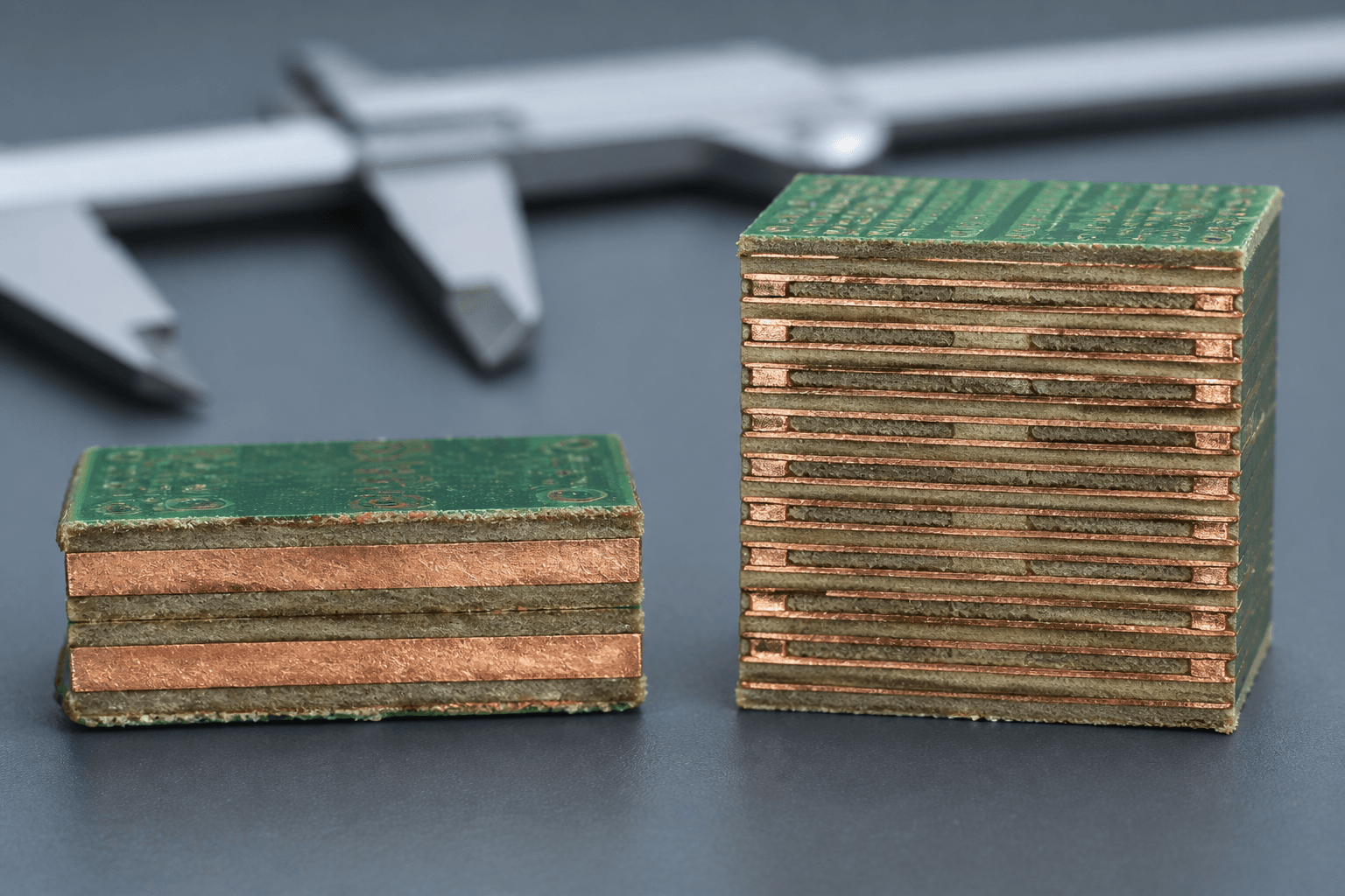
A 40-layer 112G board is a different profession than a 4-layer shield. How to hire the high-speed PCB and signal-integrity engineer your product needs.
"PCB designer" covers a range of skill so wide that the title is almost meaningless on its own. The person who can lay out a 4-layer sensor board and the person who can design a 40-layer switch board with 112G channels are, in practice, in different professions. Hiring as if they are interchangeable is how a high-speed board ends up with eye diagrams that will not close and a respin nobody planned for.
The Complexity Tiers Nobody Spells Out
Board design sorts into tiers. Consumer and IoT boards are 4 to 8 layers at moderate speeds, where many engineers can deliver. High-speed digital boards run 12 to 20-plus layers with DDR5 and PCIe Gen5 interfaces and require real signal-integrity expertise. Datacenter, networking, and HPC boards reach 20 to 40-plus layers with multi-gigabit channels, advanced low-loss materials, and high-density BGA fanout, and that is a small, elite pool. RF and microwave is a separate discipline again. Knowing which tier your product sits in is the first step to hiring for it.
High-Speed Is a Different Profession
Once you are routing DDR5, PCIe Gen5/Gen6, or the kind of multi-gigabit channels heading toward 800G Ethernet (IEEE 802.3df) and OIF's CEI-224G, the work changes character. Stackup design, controlled impedance, low-loss dielectrics, and dense BGA fanout stop being optional refinements and become the core of the job. An engineer who has only done lower-tier work will not have these skills, and the board will tell you so at bring-up.
SI/PI Is Where Boards Succeed or Fail
On high-speed boards, signal integrity and power integrity analysis is not a separate luxury role; it is how the board works at all. The engineer (or the SI specialist they work with) simulates the channel, validates the eye diagram, and designs the power delivery network with tools like Siemens HyperLynx, Cadence Sigrity, Ansys HFSS, or Keysight ADS. If a candidate cannot speak to eye diagrams and PDN impedance, they are not a high-speed hire, whatever the layer count on their last board.
Tools and Outputs That Signal Depth
The credible toolchain is Cadence Allegro, Altium Designer, or Siemens Xpedition for design and layout, plus an SI/PI tool for high-speed analysis. On the output side, fluency with manufacturing data formats, including the IPC-2581 (IPC-DPMX) standard as well as Gerber and ODB++, signals an engineer who has actually shipped boards to fabrication, not just drawn them.
The Bring-Up Test
Design is half the job. The other half is powering up the first board and making it work: probing signals, validating interfaces, and debugging the problems that only appear in copper. Ask a candidate to walk through a board bring-up that went sideways and how they isolated the cause. The answer separates engineers who design boards from engineers who deliver working hardware.
How Game 7 Places Board and SI Engineers
Game 7 recruits exclusively in semiconductor and hardware, so we match board engineers (from our vetted network of 50,000+ engineers who've shipped) to the actual complexity tier of your product, not just the title. Whether you need a high-speed layout engineer, a signal-integrity specialist, or a hardware engineer who can own bring-up, submit your hiring needs and we will put the right tier of talent in front of you so you can make a choice from 2-3 qualified engineers, instead of 10-15 resumes matched by keywords.
FAQ
Frequently Asked Questions
What's the difference between a PCB designer and a high-speed board engineer?
Layer count and signal speed. A 4 to 8-layer consumer board and a 20 to 40-layer datacenter board with 112G channels require very different skills, including impedance control, stackup design, and signal-integrity analysis that most generalist PCB designers have never done.
When do I need a signal integrity engineer?
When you have DDR5, PCIe Gen5/Gen6, or multi-gigabit SerDes channels. Those interfaces need impedance-controlled routing and eye-diagram validation, which a dedicated SI engineer using HyperLynx, Sigrity, HFSS, or ADS provides.
Which tools should a high-speed PCB engineer know?
Cadence Allegro, Altium Designer, or Siemens Xpedition for design and layout, plus an SI/PI tool such as HyperLynx, Sigrity, HFSS, or ADS for high-speed analysis, and fluency with output formats like IPC-2581, Gerber, and ODB++.
Can board design and bring-up be done on contract?
Yes. Contract hardware and SI engineers are commonly placed for a specific board spin and bring-up window, which fits the time-boxed nature of a hardware program.
Written by
Game 7 Staff